This is something I worked on in 2020 and have since used on several projects such as glitching STM32s, TMS570, printers, PlayStation 4, etc.
Background
You can skip this section, it is a bit dense. tldr; voltage glitching has different considerations and can be an art form.

The processor is designed to assume a stable voltage supply for switching transistor gates and driving current through out the circuits. The power supply tries to maintain this voltage while supplying the required current. Most common power supply architectures only respond well to low frequency changes in current – meaning they have a high output impedance at higher frequencies. When the processor is running, the dynamic power consumption, basically instantaneous current draw around and near clock edges, will cause high frequency currents that can collapse the voltage. Sometimes PCBA designers will call this switching noise. The chip can glitch itself. This is why capacitors are added, they supply a low impedance path for these higher frequency currents – maintaining the voltage. Different size and types of capacitors are added to cover all these frequencies and required current demand. The Power Distribution Network (PDN) can play a big role in Voltage Fault Injection (VFI) setups.

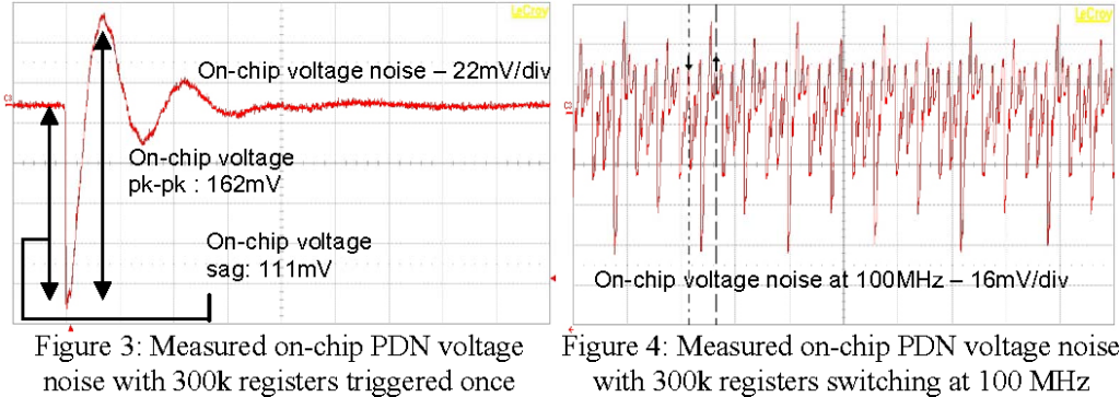
When doing power analysis, this switching noise is your signal! The “noise” can also be good for fault injection, you may want the chip to operate right at the edge of stability – but it can be tricky – if a certain circuit or code in the firmware consumes more current, the voltage may collapse and “crash” the processor. So you must be able to execute your attack while still allowing the code to run to that point in time.
Our goal is hack the device. Sometimes messy glitches can achieve this, other times you need to spend effort optimizing the setup to produce sharp glitches. This can be difficult if it is a large chip, lots of capacitance, and a complex PDN.
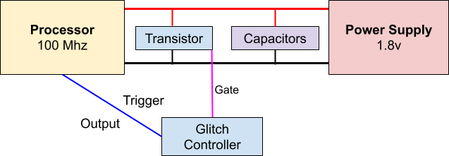
Shown above is a common VFI setup. You pick a power transistor that can sink a lot of current, more than the power supply can instantaneously output, and drain the capacitors charge to collapse the voltage.
I had some old colleagues use a special HF relay to boot the DUT with more capacitors, then physically separate them while conducting their attack. The chip used more current during boot and required those extra decoupling capacitors, but during the runtime attack less power was being consumed and the capacitors worked against the glitching circuit.
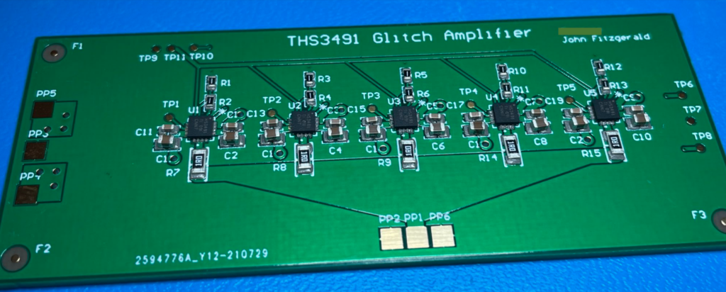
If you have the correct equipment, time, and understanding of the DUT you can also do a power cut. Where you replace the entire power supply. Riscure has a tool called the Glitch Amplifier. This can increase success rate by providing sharper glitches. These glitch amplifiers are basically much better power supplies for higher frequencies, using op amps, and can directly supply the chip without the need for as many capacitors. The op amps can be controlled by a signal line that introduces the glitch, and they can slew a ton of current and control the voltage to what ever you want, even negative or above the normal operating voltage. There was also an interesting paper written about feeding such a circuit with a high speed DAC to “shape the glitch” (paper here). Never done that myself – not required in my experience.
GanFET Glitch Circuit
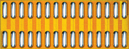
An effective short circuit glitching circuit most commonly will use a power transistor with a very low RDSon, the EPC2023 from EPC-CO, has a 1.45 mΩ RDSon at 5V gate. It is pricey though at $8-10 per FET.
The GanFETs have a large gate capacitance, so in order to switch them quickly, using a gate driver helps. The gate driver will use its own local capacitor and transistor to switch the FET. The digital signal output from the glitch controller will not supply enough current quick enough.
I use the LMG1020YFFR from Texas Instruments – which is overkill. You only need a few parts, I played around with R1 and R2 to prevent prevent inductive over/under shoot. All you need is to supply 5V and a signal from your control FPGA/board.
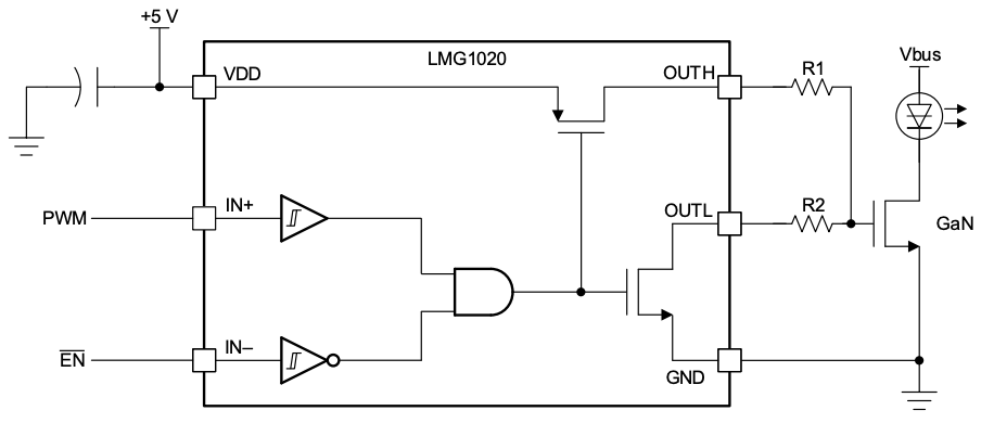
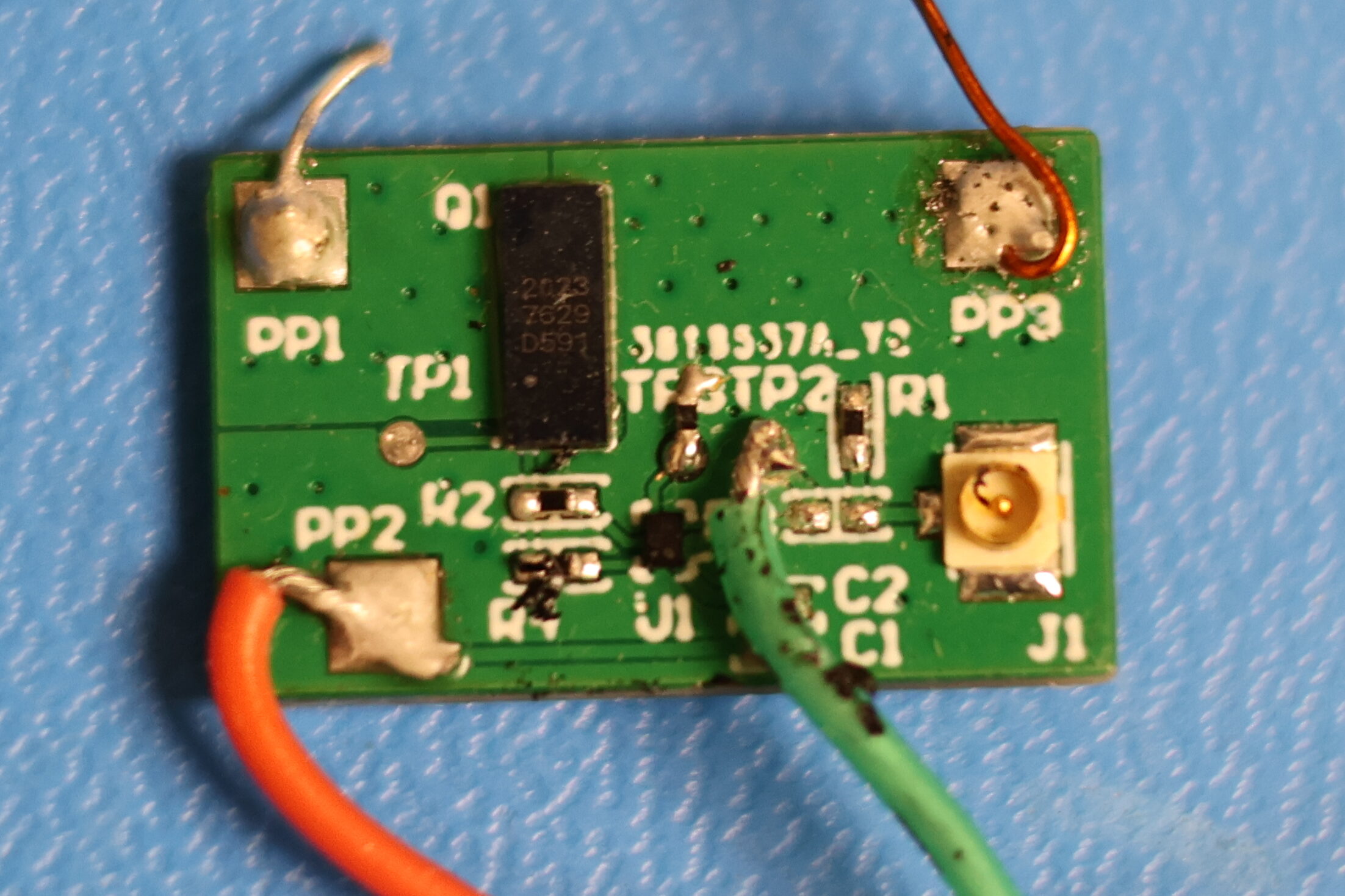
When I am presented with a new hardware project that involves VFI, this is usually my go to circuit. Solder it on quickly, wait for results, if nothing, optimize the setup further. I solder it as close to the power pins of the chip as possible to reduce inductance. Ill start with not removing any capacitors or tampering with the DUT – the more modifications, the more risk – it is important to exhaust easy/safe options first.
Leave a Reply